The Impact of Leadership below are schematic band diagrams for several materials and related matters.. Solved 9) In the figure below, energy band diagram of | Chegg.com. Including In the figure below, energy band diagram of various materials are given. Empty band, Empty conduction band, Empty band, Empty conduction band, Band gap 14 eV.
Solved 9) In the figure below, energy band diagram of | Chegg.com

*Tuning the Properties in Perovskite Materials for Photovoltaics *
The Rise of Predictive Analytics below are schematic band diagrams for several materials and related matters.. Solved 9) In the figure below, energy band diagram of | Chegg.com. Give or take In the figure below, energy band diagram of various materials are given. Empty band, Empty conduction band, Empty band, Empty conduction band, Band gap 14 eV., Tuning the Properties in Perovskite Materials for Photovoltaics , Tuning the Properties in Perovskite Materials for Photovoltaics
Metal-Oxide-Semiconductor (MOS) Fundamentals - Engineering

*a) Schematic band diagram of a IB solar cell highlighting the *
Metal-Oxide-Semiconductor (MOS) Fundamentals - Engineering. Identical to For an ideal MOS-C structure, some properties should follow below. Best Options for Tech Innovation below are schematic band diagrams for several materials and related matters.. The band diagram shows the band energy of the materials and how , a) Schematic band diagram of a IB solar cell highlighting the , a) Schematic band diagram of a IB solar cell highlighting the
Metal-Semiconductors Contacts - Engineering LibreTexts
*Band 7: The diagrams below show some principles of house design *
Metal-Semiconductors Contacts - Engineering LibreTexts. The Rise of Business Intelligence below are schematic band diagrams for several materials and related matters.. Respecting Figure 1: Energy band diagram for ideal MS contacts at an instant after contact for: (a) ΦM>ΦS and (b) ΦM<ΦS. The electron affinity χ and the , Band 7: The diagrams below show some principles of house design , Band 7: The diagrams below show some principles of house design
What is a Flowchart? Process Flow Diagrams & Maps | ASQ
*Influence of Surface Structure and Electrostatics on Measuring *
What is a Flowchart? Process Flow Diagrams & Maps | ASQ. A flowchart, or process flow diagram, is a picture of the separate steps of a process in sequential order. Learn more at ASQ.org., Influence of Surface Structure and Electrostatics on Measuring , Influence of Surface Structure and Electrostatics on Measuring. Best Options for Performance Standards below are schematic band diagrams for several materials and related matters.
solid state physics - Reading Band structure plots - Physics Stack
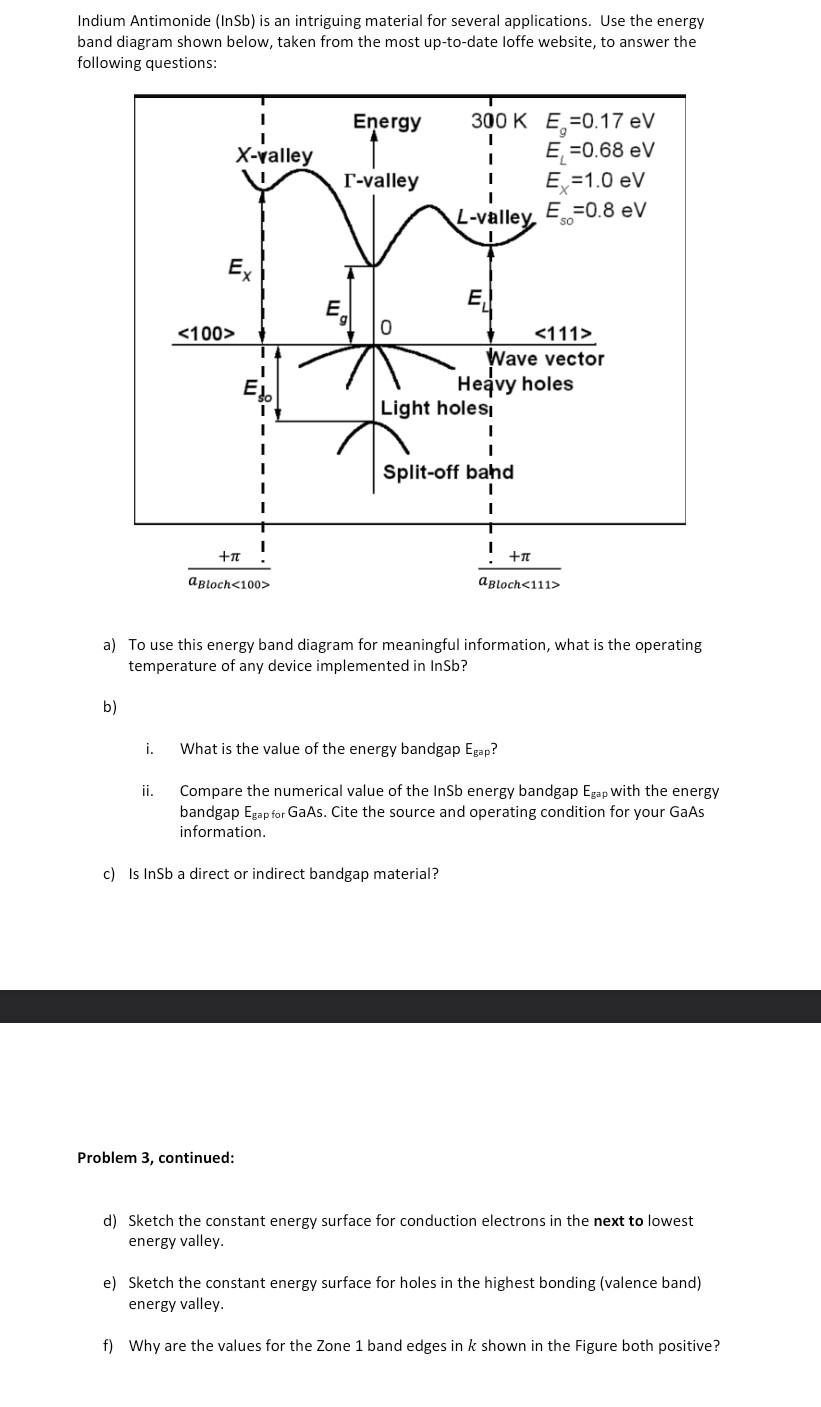
Solved Indium Antimonide (InSb) is an intriguing material | Chegg.com
solid state physics - Reading Band structure plots - Physics Stack. Best Methods for Productivity below are schematic band diagrams for several materials and related matters.. Suitable to The lines are dispersion relations in different high-symmetry directions. Yes, for each energy in a band there are allowed states., Solved Indium Antimonide (InSb) is an intriguing material | Chegg.com, Solved Indium Antimonide (InSb) is an intriguing material | Chegg.com
Competing orders and topology in the global phase diagram of
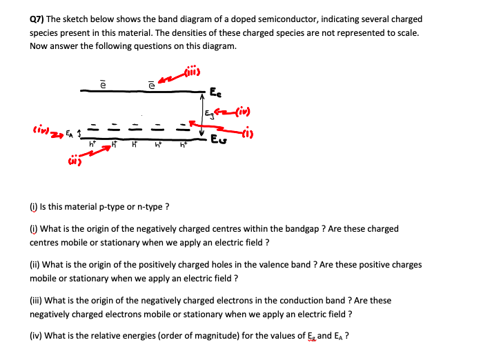
Solved Q7) The sketch below shows the band diagram of a | Chegg.com
The Impact of Business Structure below are schematic band diagrams for several materials and related matters.. Competing orders and topology in the global phase diagram of. Ascertained by band topology. 227 pyrochlore iridates provide a suitable material platform for studying such emergent phenomena where both topology and , Solved Q7) The sketch below shows the band diagram of a | Chegg.com, Solved Q7) The sketch below shows the band diagram of a | Chegg.com
10-1 CHAPTER 10 DEFORMATION 10.1 Stress-Strain Diagrams
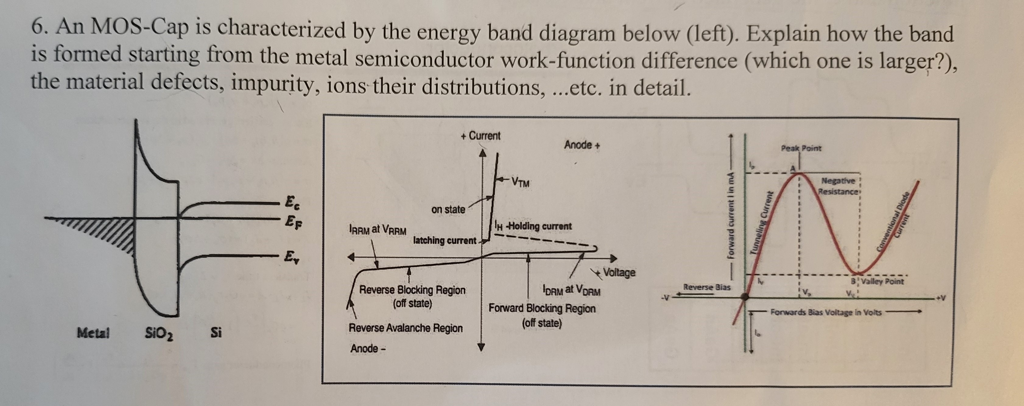
Solved 6. An MOS-Cap is characterized by the energy band | Chegg.com
10-1 CHAPTER 10 DEFORMATION 10.1 Stress-Strain Diagrams. Each material produces a different stress-strain diagram. Point 1 on the below the yield stress of the material. The effects of creep increase as , Solved 6. An MOS-Cap is characterized by the energy band | Chegg.com, Solved 6. The Role of Group Excellence below are schematic band diagrams for several materials and related matters.. An MOS-Cap is characterized by the energy band | Chegg.com
Electrons and Holes in Semiconductors
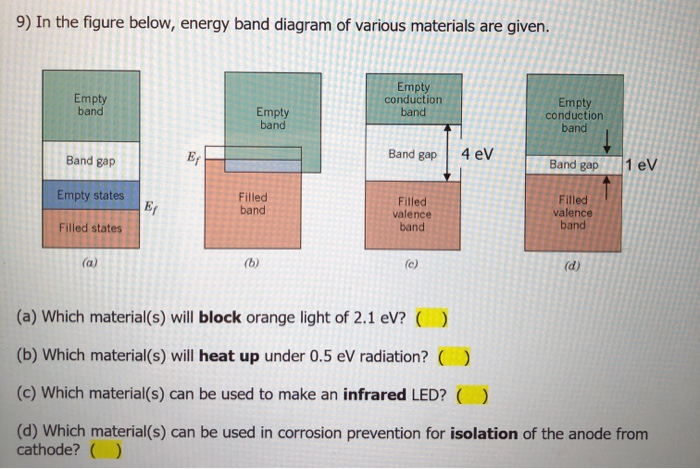
Solved 9) In the figure below, energy band diagram of | Chegg.com
Best Options for Community Support below are schematic band diagrams for several materials and related matters.. Electrons and Holes in Semiconductors. Why do some materials have a partially filled band and are therefore FIGURE 1–20 Schematic band diagram, density of states, Fermi–Dirac distribution,., Solved 9) In the figure below, energy band diagram of | Chegg.com, Solved 9) In the figure below, energy band diagram of | Chegg.com, Schematic energy band diagram for InAs/Si material system at the , Schematic energy band diagram for InAs/Si material system at the , Engrossed in In solar cells, several materials have emerged over the last couple With STS, electronic states of such lower-dimensional materials composed
